

The ZB25VQ40B of non-volatile flash memory device supports the standard Serial Peripheral Interface(SPI).Traditional SPI single bit serial input and output(Single I/O or SIO)is supported as well as optional two bit(Dual I/O or DIO)and four bit(quad I/O)serial protocols.This multiple width interface is called SPI Multi-I/O or MIO.
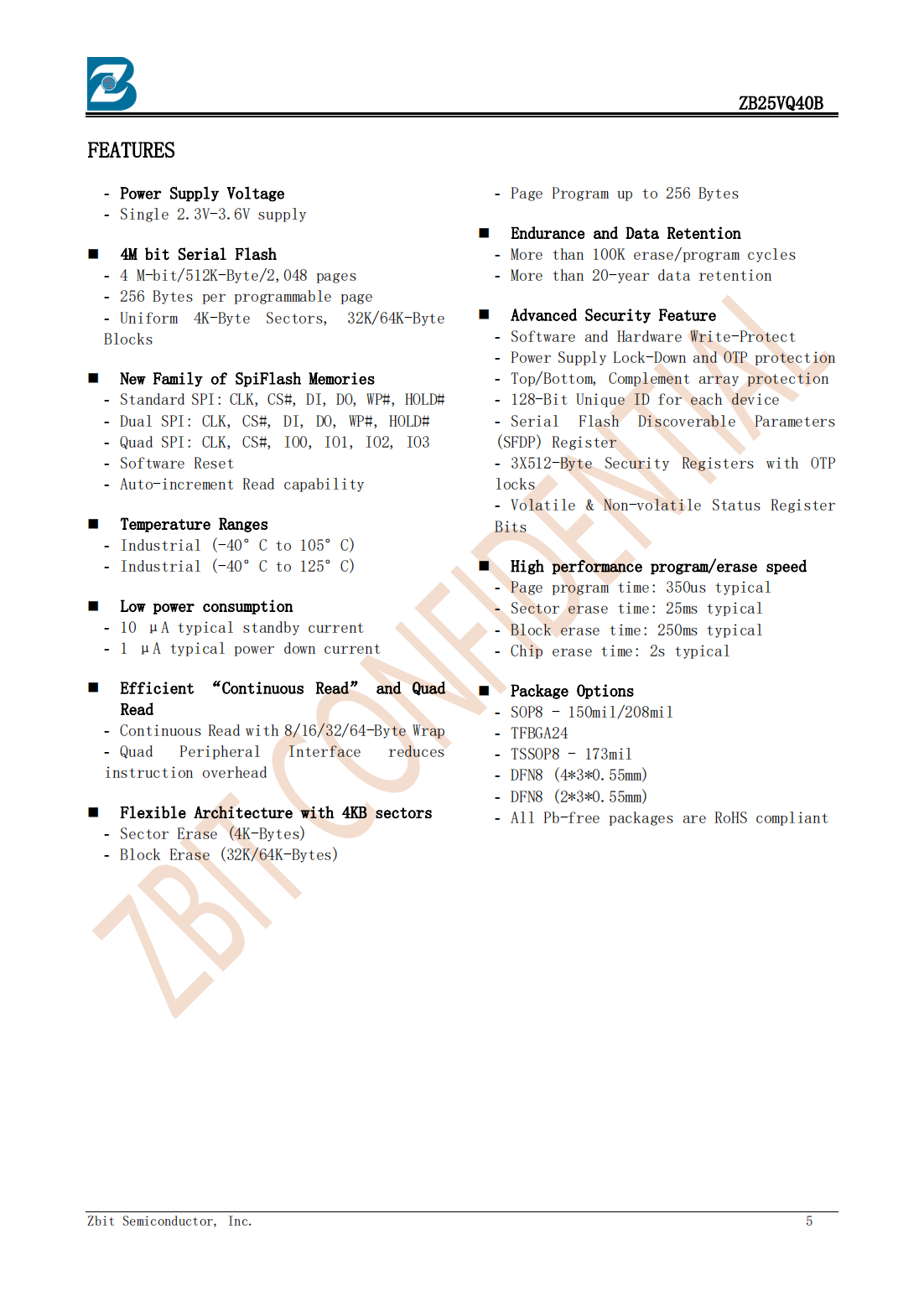
FEATURES
-Power Supply Voltage
-Single 2.3V-3.6V supply
4M bit Serial Flash
-4 M-bit/512K-Byte/2,048 pages
-256 Bytes per programmable page
-Uniform 4K-Byte Sectors,32K/64K-Byte Blocks
New Family of SpiFlash Memories
-Standard SPI:CLK,CS#,DI,DO,WP#,HOLD#
-Dual SPI:CLK,CS#,DI,DO,WP#,HOLD#
-Quad SPI:CLK,CS#,IO0,IO1,IO2,IO3
-Software Reset
-Auto-increment Read capability
Temperature Ranges
-Industrial(-40°C to 105°C)
-Industrial(-40°C to 125°C)
Low power consumption
-10μA typical standby current
-1μA typical power down current
Efficient“Continuous Read”and Quad Read
-Continuous Read with 8/16/32/64-Byte Wrap
-Quad Peripheral Interface reduces instruction overhead
Flexible Architecture with 4KB sectors
-Sector Erase(4K-Bytes)
-Block Erase(32K/64K-Bytes)
-Page Program up to 256 Bytes
Endurance and Data Retention
-More than 100K erase/program cycles
-More than 20-year data retention
Advanced Security Feature
-Software and Hardware Write-Protect
-Power Supply Lock-Down and OTP protection
-Top/Bottom,Complement array protection
-128-Bit Unique ID for each device
-Serial Flash Discoverable Parameters (SFDP)Register
-3X512-Byte Security Registers with OTP locks
-Volatile&Non-volatile Status Register Bits
High performance program/erase speed
-Page program time:350us typical
-Sector erase time:25ms typical
-Block erase time:250ms typical
-Chip erase time:2s typical
Package Options
-SOP8-150mil/208mil
-TFBGA24
-TSSOP8-173mil
-DFN8(4*3*0.55mm)
-DFN8(2*3*0.55mm)
-All Pb-free packages are RoHS compliant


 18677706250
 咨询
咨询